- 您现在的位置:买卖IC网 > Sheet目录3827 > PIC16F877A-I/P (Microchip Technology)IC MCU FLASH 8KX14 EE 40DIP
PIC18F2525/2620/4525/4620
DS39626E-page 214
2008 Microchip Technology Inc.
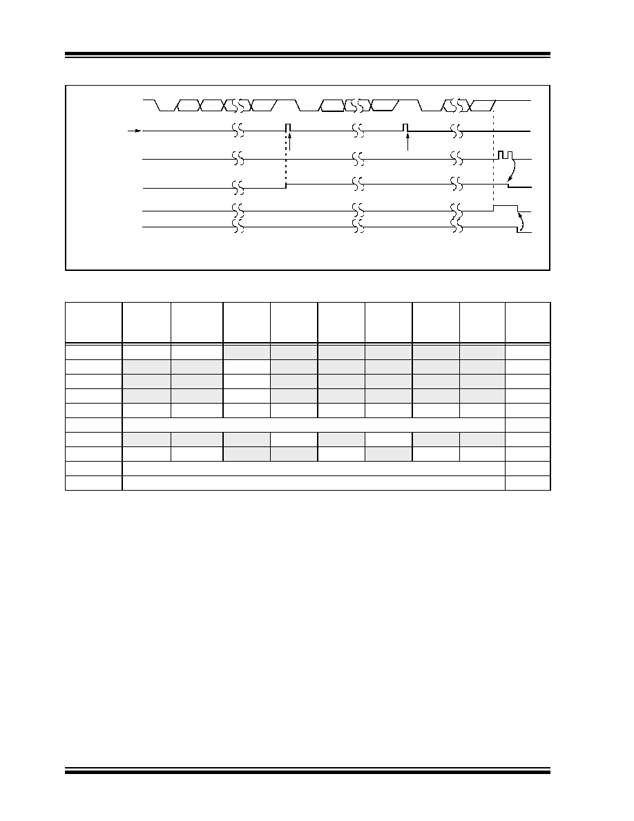
FIGURE 18-7:
ASYNCHRONOUS RECEPTION
TABLE 18-6:
REGISTERS ASSOCIATED WITH ASYNCHRONOUS RECEPTION
18.2.4
AUTO-WAKE-UP ON SYNC
BREAK CHARACTER
During Sleep mode, all clocks to the EUSART are
suspended. Because of this, the Baud Rate Generator
is inactive and a proper byte reception cannot be per-
formed. The auto-wake-up feature allows the controller
to wake-up due to activity on the RX/DT line while the
EUSART is operating in Asynchronous mode.
The auto-wake-up feature is enabled by setting the
WUE bit (BAUDCON<1>). Once set, the typical receive
sequence on RX/DT is disabled and the EUSART
remains in an Idle state, monitoring for a wake-up event
independent of the CPU mode. A wake-up event
consists of a high-to-low transition on the RX/DT line.
(This coincides with the start of a Sync Break or a
Wake-up Signal character for the LIN protocol.)
Following a wake-up event, the module generates an
RCIF interrupt. The interrupt is generated synchro-
nously to the Q clocks in normal operating modes
(Figure 18-8) and asynchronously, if the device is in
Sleep mode (Figure 18-9). The interrupt condition is
cleared by reading the RCREG register.
The WUE bit is automatically cleared once a low-to-
high transition is observed on the RX line following the
wake-up event. At this point, the EUSART module is in
Idle mode and returns to normal operation. This signals
to the user that the Sync Break event is over.
Name
Bit 7
Bit 6
Bit 5
Bit 4
Bit 3
Bit 2
Bit 1
Bit 0
Reset
Values
on page
INTCON
GIE/GIEH PEIE/GIEL
TMR0IE
INT0IE
RBIE
TMR0IF
INT0IF
RBIF
PIR1
PSPIF(1)
ADIF
RCIF
TXIF
SSPIF
CCP1IF
TMR2IF
TMR1IF
PIE1
PSPIE(1)
ADIE
RCIE
TXIE
SSPIE
CCP1IE
TMR2IE
TMR1IE
IPR1
PSPIP(1)
ADIP
RCIP
TXIP
SSPIP
CCP1IP
TMR2IP
TMR1IP
RCSTA
SPEN
RX9
SREN
CREN
ADDEN
FERR
OERR
RX9D
RCREG
EUSART Receive Register
TXSTA
CSRC
TX9
TXEN
SYNC
SENDB
BRGH
TRMT
TX9D
BAUDCON
ABDOVF
RCIDL
RXDTP
TXCKP
BRG16
—
WUE
ABDEN
SPBRGH
EUSART Baud Rate Generator Register High Byte
SPBRG
EUSART Baud Rate Generator Register Low Byte
Legend: — = unimplemented locations read as ‘0’. Shaded cells are not used for asynchronous reception.
Note 1:
These bits are unimplemented on 28-pin devices and read as ‘0’.
Start
bit
bit 7/8
bit 1
bit 0
bit 7/8
bit 0
Stop
bit
Start
bit
Start
bit
bit 7/8
Stop
bit
RX (pin)
Rcv Buffer Reg
Rcv Shift Reg
Read Rcv
Buffer Reg
RCREG
RCIF
(Interrupt Flag)
OERR bit
CREN
Word 1
RCREG
Word 2
RCREG
Stop
bit
Note:
This timing diagram shows three words appearing on the RX input. The RCREG (receive buffer) is read after the third word causing
the OERR (overrun) bit to be set.
发布紧急采购,3分钟左右您将得到回复。
相关PDF资料
MP2-HS240-51
CONN SHROUD 2-FB 240POS 5ROW
DSPIC33FJ64MC506-I/PT
IC DSPIC MCU/DSP 64K 64TQFP
DSPIC33FJ128MC802-I/SO
IC DSPIC MCU/DSP 128K 28SOIC
PIC18LF4331-I/P
IC PIC MCU FLASH 4KX16 40DIP
DSPIC33FJ128GP306-I/PT
IC DSPIC MCU/DSP 128K 64TQFP
PIC24HJ128GP306-I/PT
IC PIC MCU FLASH 128KB 64TQFP
PIC16F873-20/SO
IC MCU FLASH 4KX14 EE 28SOIC
PIC18F4431-I/P
IC PIC MCU FLASH 8KX16 40DIP
相关代理商/技术参数
PIC16F877A-I/P
制造商:Microchip Technology Inc 功能描述:IC 8BIT FLASH MCU 16F877 DIP40
PIC16F877A-I/PG
功能描述:8位微控制器 -MCU 14KB 368 RAM 33 I/O RoHS:否 制造商:Silicon Labs 核心:8051 处理器系列:C8051F39x 数据总线宽度:8 bit 最大时钟频率:50 MHz 程序存储器大小:16 KB 数据 RAM 大小:1 KB 片上 ADC:Yes 工作电源电压:1.8 V to 3.6 V 工作温度范围:- 40 C to + 105 C 封装 / 箱体:QFN-20 安装风格:SMD/SMT
PIC16F877A-I/PT
功能描述:8位微控制器 -MCU 14KB 368 RAM 33 I/O RoHS:否 制造商:Silicon Labs 核心:8051 处理器系列:C8051F39x 数据总线宽度:8 bit 最大时钟频率:50 MHz 程序存储器大小:16 KB 数据 RAM 大小:1 KB 片上 ADC:Yes 工作电源电压:1.8 V to 3.6 V 工作温度范围:- 40 C to + 105 C 封装 / 箱体:QFN-20 安装风格:SMD/SMT
PIC16F877A-I/PT
制造商:Microchip Technology Inc 功能描述:8BIT FLASH MCU SMD 16F877 TQFP44
PIC16F877A-I/PTG
功能描述:8位微控制器 -MCU 14KB 368 RAM 33 I/O RoHS:否 制造商:Silicon Labs 核心:8051 处理器系列:C8051F39x 数据总线宽度:8 bit 最大时钟频率:50 MHz 程序存储器大小:16 KB 数据 RAM 大小:1 KB 片上 ADC:Yes 工作电源电压:1.8 V to 3.6 V 工作温度范围:- 40 C to + 105 C 封装 / 箱体:QFN-20 安装风格:SMD/SMT
PIC16F877AIL
制造商:Microchip Technology Inc 功能描述:
PIC16F877AIP
制造商:Microchip Technology Inc 功能描述:
PIC16F877AIPT
制造商:Microchip Technology Inc 功能描述: